PCB Assembly for Tech Gifts: Solder Paste Stencil Alignment Tolerance and Defect Prevention
When a corporate client orders 5,000 custom-branded power banks or USB drives, they're rarely thinking about the PCB assembly process that makes those devices functional. Yet the technical precision required to reliably solder dozens of tiny surface-mount components onto a circuit board—components often smaller than a grain of rice—is what separates a functional promotional product from an expensive paperweight. The critical first step in this process is solder paste stencil printing, where a thin metal stencil is used to deposit precise amounts of solder paste onto PCB pads before component placement and reflow soldering.
Having troubleshot countless SMT (Surface Mount Technology) assembly lines producing promotional electronics across Southeast Asia, I've seen how stencil alignment errors cascade into systematic defects: solder bridges shorting adjacent pins, tombstoned components standing on end instead of lying flat, insufficient solder joints that fail electrical testing, or excessive solder creating messy, unprofessional-looking boards. The challenge isn't just "printing solder paste"—it's achieving sub-50-micron alignment accuracy, controlling paste rheology to prevent slumping or spreading, and designing stencil apertures that deposit the right volume of paste for each component type.
The Stencil: Precision Metal Fabrication for Microscopic Accuracy
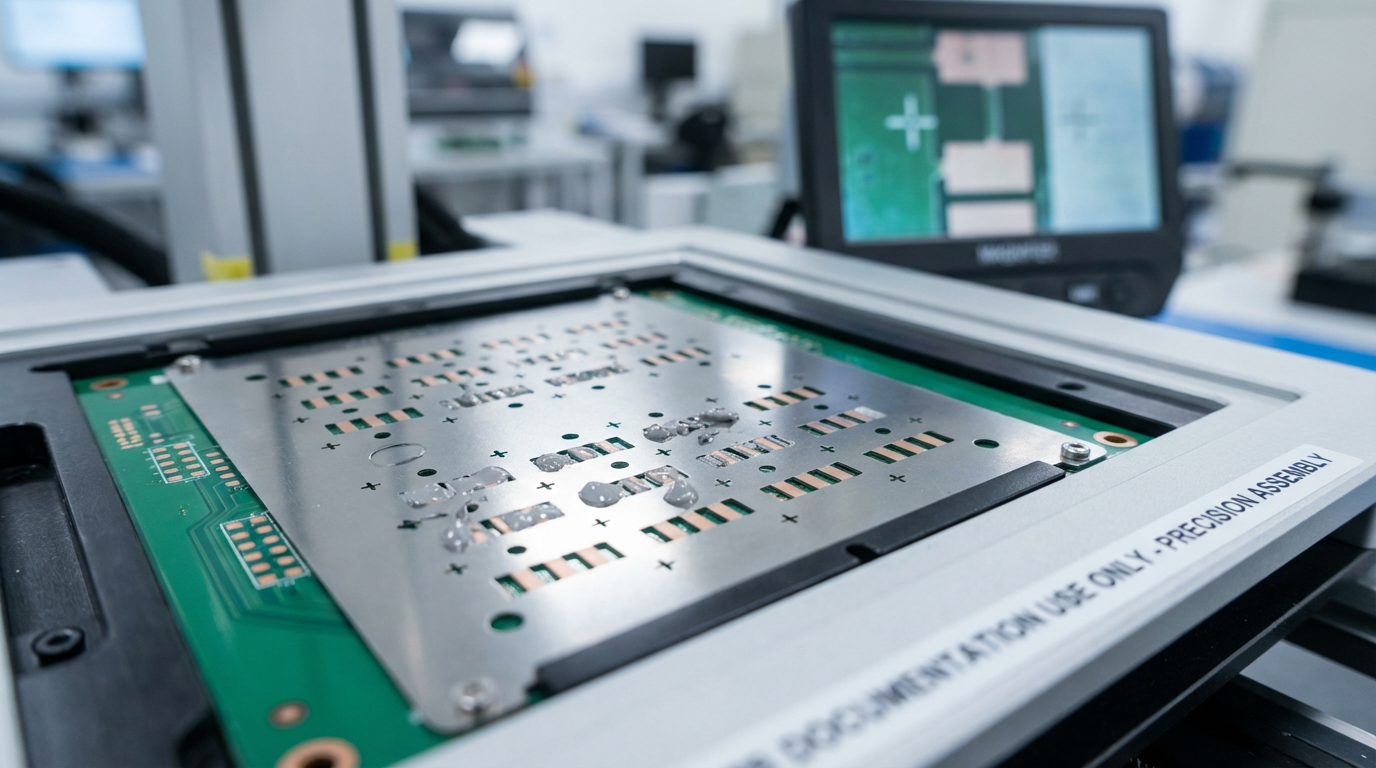
A solder paste stencil is essentially a thin metal sheet (typically stainless steel) with precisely cut openings (apertures) that correspond to the solder pads on the PCB. The stencil is aligned over the bare PCB, solder paste is spread across the stencil surface with a squeegee, and the paste is forced through the apertures onto the pads below. When the stencil is lifted, each pad should have a uniform deposit of solder paste with well-defined edges and consistent height.
Stencil thickness is the first critical parameter. For most promotional electronics (which use 0603, 0402, or 0201 sized SMD components), the standard stencil thickness is 100-150 microns (0.1-0.15mm). Thicker stencils deposit more solder paste, which is necessary for larger components or components with higher thermal mass (like power MOSFETs or voltage regulators). Thinner stencils deposit less paste, which is required for ultra-fine-pitch components (0.4mm or 0.5mm pitch BGAs or QFNs) to prevent solder bridging.
The aperture design is equally critical. For most rectangular SMD pads, the stencil aperture is slightly smaller than the pad itself—typically 90-95% of the pad width and length. This ensures that the solder paste deposits entirely onto the pad without spreading onto the solder mask, which would cause bridging or contamination. For very fine-pitch components (0.5mm pitch or less), the aperture may be reduced to 80-85% of pad size, and the stencil thickness may be reduced to 80-100 microns to prevent excessive paste volume.
Stencil fabrication methods also matter. Laser-cut stencils offer the tightest tolerances (±10 microns) and smoothest aperture walls, which improves paste release and deposit uniformity. Chemically-etched stencils are cheaper but have rougher aperture walls and wider tolerances (±25 microns), which can cause paste to stick in the aperture or deposit unevenly. For high-volume production of promotional electronics, laser-cut stencils are standard.
Alignment Tolerance: The 50-Micron Rule
Stencil-to-PCB alignment is measured as the maximum offset between the stencil aperture centerline and the PCB pad centerline. Industry standards specify that this offset should be less than 25% of the pad width for reliable solder joint formation. For a typical 0603 component with a 0.8mm x 0.8mm pad, this means the alignment tolerance is ±0.2mm (200 microns). However, for modern fine-pitch components (0.5mm pitch QFNs or 0.4mm pitch BGAs), the tolerance tightens to ±50 microns or less.
Achieving this level of alignment requires automated vision systems. Manual stencil alignment (using tooling pins or visual reference marks) can achieve ±100-150 microns at best, which is inadequate for fine-pitch components. Automated stencil printers use cameras to locate fiducial marks on both the stencil and the PCB, calculate the offset, and adjust the stencil position using servo-controlled X-Y stages. High-end printers can achieve ±25 micron alignment repeatability, which is necessary for 0.4mm pitch components.
Misalignment manifests in predictable ways. If the stencil is offset in the X-direction, one side of each pad will have excess solder paste (which can cause bridging to adjacent pads), while the opposite side will have insufficient paste (which can cause weak or missing solder joints). If the stencil is rotated (theta error), the misalignment will be worse at the corners of the board than at the center, causing corner components to have more defects.
One subtle issue is PCB warpage. If the PCB isn't perfectly flat, the stencil won't make uniform contact across the entire board surface. Areas where the PCB is bowed upward will have poor stencil contact, resulting in incomplete paste deposits or smeared paste edges. Areas where the PCB is bowed downward will have excessive stencil contact, potentially causing paste to be forced under the stencil edges and contaminate adjacent areas. To prevent this, stencil printers use vacuum hold-down systems to flatten the PCB against the print table before printing.
Solder Paste Rheology: Viscosity, Slump, and Tack Life
Solder paste is a complex mixture of tiny solder alloy particles (typically 25-45 microns diameter) suspended in a flux medium. The flux serves multiple purposes: it suspends the solder particles, provides tackiness to hold components in place before reflow, and chemically cleans the pad surfaces during reflow to promote solder wetting. The rheological properties of this mixture—how it flows under shear stress and how it behaves after printing—are critical to print quality.
Solder paste viscosity is typically specified at a shear rate of 10 s⁻¹ (simulating the squeegee action) and ranges from 150-250 Pa·s for most SMT applications. Paste that's too thin (low viscosity) will slump after printing, spreading beyond the pad edges and causing bridging. Paste that's too thick (high viscosity) won't release cleanly from the stencil apertures, resulting in incomplete deposits or "dog-earing" (paste sticking to the aperture walls and pulling away from the pad).
Paste viscosity is temperature-dependent—it decreases as temperature increases. This is why stencil printing is typically done in climate-controlled environments (22-25°C, 40-60% RH). If the production floor is too hot (>28°C), the paste becomes too thin and slumps. If it's too cold (<20°C), the paste becomes too thick and doesn't print cleanly. Humidity also matters: low humidity (<30% RH) causes the flux solvents to evaporate too quickly, increasing viscosity and reducing tack life. High humidity (>70% RH) can cause moisture absorption, which leads to solder balling defects during reflow.
Tack life is the time window after printing during which the paste retains sufficient stickiness to hold components in place during pick-and-place assembly. Most solder pastes have a tack life of 30-60 minutes at 22°C. After this time, the flux solvents evaporate, the paste dries out, and components may shift or fall off during board handling. For high-volume production, this means the time from stencil printing to reflow oven entry must be tightly controlled—boards that sit too long between printing and reflow will have higher defect rates.
Squeegee Parameters: Speed, Pressure, and Angle
The squeegee blade is what forces solder paste through the stencil apertures. Squeegee parameters—blade material, speed, pressure, and angle—all affect print quality.
Blade material is typically either metal (stainless steel) or polyurethane. Metal blades are more durable and provide more consistent pressure across the stencil, but they can damage delicate stencil features if the pressure is too high. Polyurethane blades are softer and more forgiving, but they wear faster and can cause uneven pressure distribution as they deform under load. For fine-pitch printing, metal blades are preferred for their consistency.
Squeegee speed is typically 20-50 mm/s. Slower speeds allow more time for the paste to flow into the apertures, which improves fill for small apertures but increases the risk of paste spreading under the stencil edges. Faster speeds reduce print time but can cause incomplete aperture fill, especially for small or deep apertures (high aspect ratio). The optimal speed depends on the paste viscosity and the smallest aperture size on the stencil.
Squeegee pressure is typically 0.3-0.5 kg/cm of blade length. Too little pressure causes incomplete aperture fill and paste residue left on the stencil surface. Too much pressure forces paste under the stencil edges, causing smearing and contamination. Pressure must be balanced with blade angle—a blade held at 60° requires less pressure than a blade held at 45° to achieve the same contact force.
One often-overlooked parameter is the squeegee stroke length. The squeegee should travel at least 25mm beyond the last aperture before stopping, to ensure that paste is fully cleared from the stencil surface. If the squeegee stops too soon, residual paste can drip onto the board or contaminate the next print cycle.
Common Defects and Root Causes
Solder Bridging: Excess solder paste between adjacent pads, causing electrical shorts. Root causes: stencil apertures too large, stencil misalignment, paste slumping due to low viscosity or high temperature, or excessive squeegee pressure forcing paste under stencil edges.
Insufficient Solder (Cold Joints): Weak or incomplete solder joints that fail electrical testing. Root causes: stencil apertures too small, incomplete aperture fill due to high paste viscosity or fast squeegee speed, stencil misalignment causing partial pad coverage, or paste drying out before reflow (exceeded tack life).
Tombstoning: Components standing on end instead of lying flat after reflow. Root causes: uneven solder paste volume on the two pads (often due to stencil misalignment), uneven heating during reflow causing one pad to melt before the other, or component placement offset.
Solder Balling: Small spheres of solder scattered around components after reflow. Root causes: paste slumping before reflow, moisture contamination in the paste, or excessive flux volatilization during reflow causing solder particles to be ejected.
Paste-in-Hole (PTH Contamination): Solder paste deposited into through-holes, causing contamination or blocking wave soldering. Root causes: stencil apertures too close to PTH pads, excessive squeegee pressure, or PCB warpage causing poor stencil contact.
Inspection and Process Control
Modern stencil printers include automated solder paste inspection (SPI) systems that use 3D laser scanning or structured light to measure the height, volume, and position of every solder paste deposit immediately after printing. This allows real-time process control—if the SPI detects that paste deposits are trending toward out-of-spec, the printer can automatically adjust squeegee pressure, speed, or stencil separation speed to bring the process back into control.
Key SPI metrics include:
- Paste height: Should be 80-120% of stencil thickness (e.g., 80-120 microns for a 100-micron stencil).
- Paste volume: Should be within ±20% of the target volume calculated from aperture size and stencil thickness.
- Paste position: Centerline offset from pad center should be less than 25% of pad width.
- Paste shape: Should have well-defined edges with minimal slumping or smearing.
For promotional electronics production, where margins are tight and rework is expensive, SPI is essential for catching defects before component placement. A board with out-of-spec paste deposits can be cleaned and reprinted in seconds. A board with soldering defects discovered after reflow requires manual rework, which costs 10-20x more in labor and often results in cosmetic damage that makes the product unsellable.
Material Considerations for Lead-Free Soldering
Most promotional electronics now use lead-free solder paste (typically SAC305: 96.5% tin, 3% silver, 0.5% copper) due to RoHS regulations. Lead-free paste has different rheological properties than traditional tin-lead paste: it's generally more viscous, has a narrower process window, and requires higher reflow temperatures (peak 245-255°C vs. 215-225°C for tin-lead).
The higher reflow temperature affects component selection—not all components can withstand 255°C peak temperature, especially plastic-encapsulated components like connectors, switches, or LEDs. This is why BOM (bill of materials) review is critical before PCB design—the assembly process engineer needs to verify that all components are rated for lead-free reflow temperatures.
Lead-free paste also has shorter tack life and is more prone to oxidation than tin-lead paste. This means the time window from printing to reflow is tighter, and boards that sit too long will have higher defect rates. For high-volume production, this often necessitates inline printing (stencil printer directly feeding the pick-and-place machine and reflow oven) rather than batch printing.
The Procurement Perspective: Evaluating Assembly Quality
When sourcing promotional electronics, the technical questions that reveal assembly process maturity are:
- What stencil thickness and aperture design rules do you use for different component types?
- What is your stencil-to-PCB alignment tolerance, and how do you verify it (manual vs. automated vision)?
- What solder paste brand and alloy do you use, and how do you control environmental conditions (temperature, humidity) during printing?
- Do you use automated solder paste inspection (SPI), and what are your acceptance criteria for paste height, volume, and position?
- What is your typical first-pass yield for SMT assembly, and what are your most common defect types?
Suppliers who can answer these questions with specific numbers and process controls are demonstrating real technical capability. Suppliers who give vague answers or claim "we follow industry standards" are likely operating with less process control and higher defect rates—which means your promotional power banks are more likely to fail in the field, damaging your brand reputation.
The difference between a reliable tech gift and a warranty nightmare often comes down to these invisible details—the 50-micron alignment tolerance, the carefully controlled paste rheology, the optimized squeegee parameters. When you're ordering custom electronics, you're not just buying components and PCBs—you're buying the accumulated knowledge of how to make microscopic solder deposits, sub-millimeter component placement, and 255°C reflow heating work together to create a functional product, thousands of times per day, with minimal variation. That's the technical foundation that makes your brand message portable and powered.
Related Articles

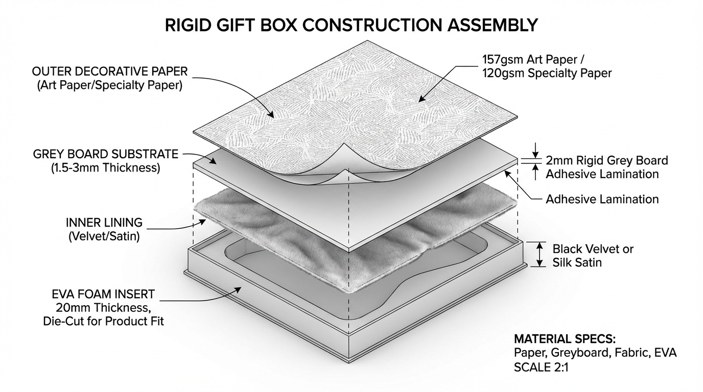
Understanding Rigid Gift Box Construction: A Material Layer Analysis for Corporate Packaging
A technical breakdown of rigid gift box construction layers, from grey board substrate to EVA foam inserts, with material specifications and assembly considerations for premium corporate packaging.

Leather Embossing Temperature Control: Why 10°C Makes the Difference Between Sharp Logos and Burnt Leather
Technical analysis of heat press temperature control in leather embossing for corporate gifts, covering brass die specifications, leather grain response, and pressure calibration for consistent branding results.

EVA Foam Insert Precision: How ±0.5mm Tolerances Affect Corporate Gift Presentation
Technical examination of die-cutting tolerances for EVA foam inserts in corporate gift packaging, covering foam density selection, cutting methods, and cavity design for secure product positioning.